I2CChip.com: PCF8574 8 Bit IO Port
| Contents
|
 Price Drop for PCF8574's and 8 bit I/O
boards! Price Drop for PCF8574's and 8 bit I/O
boards!
 |
The Philips PCF 8574 is an easy
to use 8 bit IO port chip. An advantage over many
more recent chips is 5V operation, that give you
far more drive.
- 2.5-6V supply
- 8 Open Drain I/O's with low current
pullup
- Open-Drain Interrupt Output detects pin
change
- 25mA Latched Outputs With
High-Current-Drive directly drives LEDs
- 8 addresses from 0x40 plus 8 from 0x70
We have 2 simple modules to make them easy to
use.
 Datasheet Datasheet
Philips has released a newer version the
 PCA8574 PCA8574
|
|
 |
Keyboard + LEDs module for front panels of
instruments. A single 8574 can drive 8 LED's and
read 8 push buttons. Takes 2 sizes of push buttons,
the small ones shown, and larger 12mm buttons.
Ideal for behind Mylar front panels on 19" rack
cases.

|
|
 |
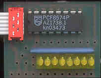
8 bit I/O module can be fitted with LED's and
external pullup resistors (needed for JLC1562) You can
fit 0.1" header pins, or SIP module pins, and just
plug it onto Veroboard for instant I/O. The power and
data are wired, you only have to connect the data pins
you want to add.
Ideal to use as an 8 LED status indicator or for
reading DIP switches. Even able to drive small relays
directly.

|
|
Very low current relays such as the NAIS TQ2-4.5V  can be driven off a single
pin. Most small 5V relays can be easily driven by just connecting
2 pins in parallel. No diode is needed as the internal diodes
suffice.
You can even drive the standard character type LCD module. See how. (Our BL301 IC
is a better way though)
As it is easy to write a series of bytes to the port, you can
easily use it to bit-bash 74HC4094's to I2C bus, or SPI chips to
the I2C bus. It won't be fast, but it works fine. Combining with
a 74HC4094 is a cheap way of interfacing an 8 bit+control lines
type peripheral to I2C. The JLC1562 won't be as
suitable for this.
Bi-color & Tri-color LEDs
Bicolor (2 pin) LEDS are driven by connecting across 2 pins of
the 8574. If one output is low, the LED will be either red or
green. Tricolor (3 pin) leds are just connected to 2 pins, with
the middle leg to ground.
Back to Top
They are incredible easy to use from the I2C-2-PC adaptor or
BL233 interface IC. Only simple ascii commands are needed, and
you can try it from the Realterm screen.
To turn an LED on we write 0 to that bit, and 1 turns it off.
So FF will be all leds off, 00 is all leds on, and FE turns led 1
on. So to turn Led 1 ON, we type:
S 40 FE P
[I2C Start][8574 Address=0x40][Data:0xFE][I2C
Stop]. The command S sends an I2C Start. P is an I2C Stop, just
like the Philips documents.
To toggle a pin or flash the LED you can just send a string of
bytes to the port:
S 40 FE FF FE FF FE P
To read 1 byte from the port
S 41 01 P (adaptor
replies with "FE")
If we are using the I2C Keyboard, then the LED and switch are
both connected to the same pin. To read the switch we turn the
LED's off (write FF), then read the buttons, then re-write the
LED's. So if LED1 of on (FE) we send.
S 40 FF R 01 W FE P (adaptor
replies with "7F" if switch 8 is pressed)
Any switch that is pressed will return 0. No switches will be
pressed will be FF.

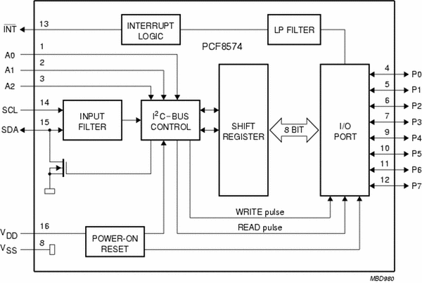
The 8574 has an 8-bit quasi-bidirectional I/O port (P0-P7),
including latched outputs with high-current-drive capability for
directly driving LEDs or small relays. Each quasi-bidirectional
I/O can be used as an input or output without the use of a
data-direction control signal.
At power on, the I/Os are high (inputs). In this mode, only a
small current source to VCC is active. An additional strong
pullup to VCC during the last clock pulse allows fast rising
edges into heavily loaded outputs. This device turns on when an
output is written high, and is switched off by the negative edge
of SCL. The I/Os should be high before being used as inputs. (You
should be aware that if the quasi bi-directional input is written
high, while it is externally being forced low, there will be a 1
clock long pulse of higher current ~1mA drawn from VCC to the
output)
The PCF8574 provides an open-drain output (INT)\ that can be
connected to the interrupt input of a microcontroller. An
interrupt is generated by any rising or falling edge of the port
inputs in the input mode. Resetting and reactivating the
interrupt circuit is achieved when data on the port is changed to
the original setting or data is read from, or written to, the
port that generated the interrupt. Resetting occurs in the read
mode at the acknowledge bit after the rising edge of the SCL
signal or in the write mode at the acknowledge bit after the
high-to-low transition of the SCL signal. Interrupts that occur
during the acknowledge clock pulse can be lost (or be very short)
due to the resetting of the interrupt during this pulse. Each
change of the I/Os after resetting is detected and, after the
next rising clock edge, is transmitted as INT\. Reading from, or
writing to, another device does not affect the interrupt circuit.
By sending an interrupt signal on this line, the remote I/O
can inform the microcontroller if there is incoming data on its
ports without having to communicate via the I2C bus. Therefore,
the PCF8574 can remain a simple slave device. (Note on the
JLC1562 this pin is the DAC output)
PCF8574's can have 8 addresses from 0x40. The PCF8574A has 8
addresses from 0x70, but is identical otherwise.
PCF8575 is a 16 bit version also at 0x40
Power On
At power on the outputs are off. That means they will be High.
Arrange your circuit so this doesn't cause a problem.
Back to Top
Alternatives:
 |
OnSemi (formerly Motorola) make a pin
compatible part that is substantially cheaper the Philips
8574. At present difficult to obtain, we expect to stock
these by March 2004.
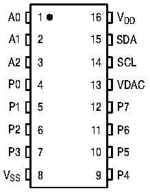
- 6 Bit DAC replaces the INT output of
PCF8574
- Address Input pins are pulled up to Vdd with
internal resistor
- I/O pins are Open Drain Outputs, but may have
lower drive (4mA @ 0.3V vs 10mA @ 1V)
- No internal pullup on I/O pins
- 5 Analog Comparator Inputs on
P0-4
- Inputs Protected from External Bus Currents in
Power Down mode
- 8 addresses from 0x70 (same as 8574A)
- 4.2-6V
 Datasheet Datasheet
|
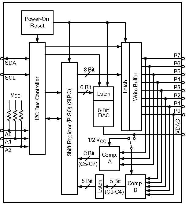
The JLC1562B facilitates easy I2C Bus expandibility. Multiple
devices (up to 8 on the same I2C Bus) are easily added as each
device has its own selectable 3-bit address. The JLC1562B
provides an 8-bit bidirectional input/output port and 6-bit
resolution Digital to Analog Converter.
The device can also be used as an Analog to Digital Converter
with 5 input signal lines each with 6-bit A/D resolution. The
voltage on pins P0-P4 is compared with the DAC voltage and the
results are readable through the I2C Bus.
The JLC1562 doesn't have internal pullups like the 8574. This
means that external pullups are needed with switches etc. Our
modules have a space for an external pullup resistor array.
The JLC1562 is slightly different for software. The second
byte written is the DAC value. This means that you can just write
a chain of bytes to the port like you can with the 8574. This
means you have to send the start and address between each byte,
so it will be slower. However it's still not difficult. With the
BL233 just use the W (write) command between values eg to send
1,2,3,4 to the port
S70 01 W 02 W 03 W 04 P

A 16 Bit version of the 8574 at address 0x40. PCF8575C has a
narrower voltage range (4.5-5.5V).
Back to Top
If you are using the surface mount parts beware:
PCF8574's are 0.3" wide packages. (normal 74XXX's are in
0.15" wide packages)
JLC1562 is in different 0.2" wide package.
sales@i2cchip.com
http://www.i2cchip.com
Phone +64 21 623-402
Please send us mail
telling us what you think about this page and how we might
improve it.


